Visible to Intel only — GUID: lro1418632211664
Ixiasoft
1.5.5.2. Hardware Design
This section presents a very simple hardware design that was used for this example. You need ACDS to be installed on your host PC to be able to reproduce this example.
Note: The design is already provided with this guide. It does not need to be re-created by the user. But it needs to be re-compiled if the Preloader hex file is changed.
The design is based on the Altera GHRD, with a reduced number of components:
- HPS - Hard Processor Instance
- SysID - System ID
- HPS Boot Memory - FPGA memory used to store Preloader binary
- Clk - Clock and Reset source
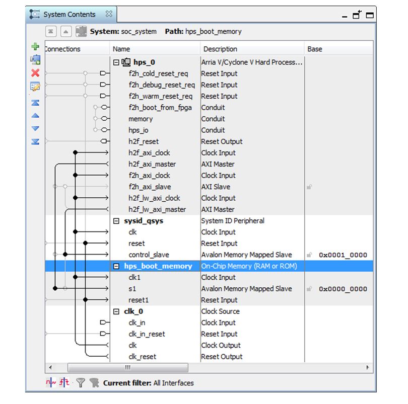
The following picture presents the System Contents view for the hardware design:
Figure 14. System Contents View for the Hardware Design
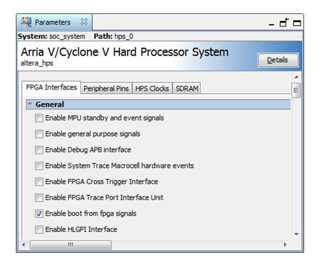
The HPS Component needs to be configured to enable the Boot from FPGA signals as shown in the screenshot below:
Figure 15. Enable Boot From FPGA Signals
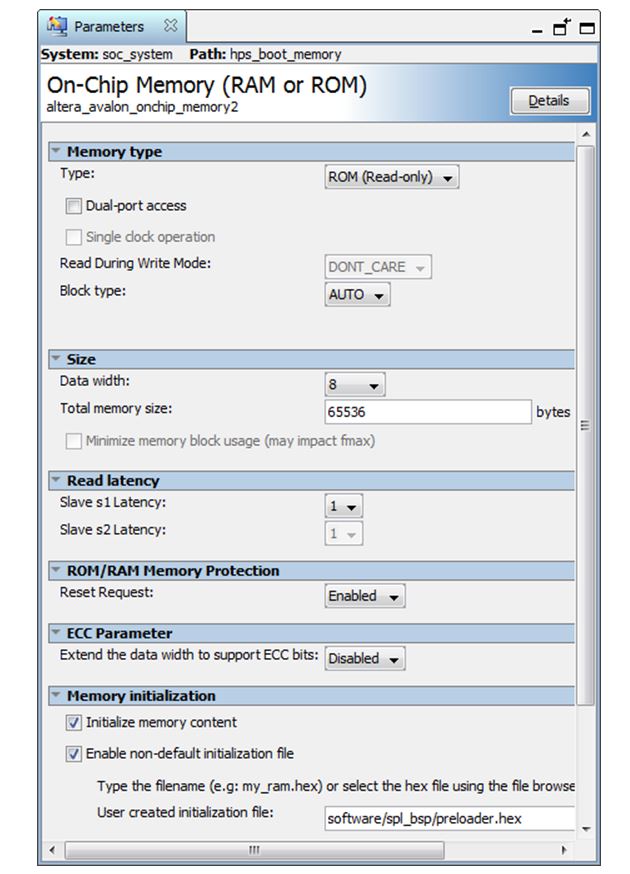
The HPS Boot Memory needs to be set to 8-bit width, and be initialized with a hex file containing the Preloader image. The following screenshot show the memory settings that were used for this example.
Note: The Preloader image is stored in the file named software/spl_bsp/preloader.hex.
Figure 16. On-Chip Memory Parameters
Note:
- The HPS bus f2h_boot_from_fpga was exported by double-clicking the corresponding cell in the Export column.
- The HPS Boot Memory was connected to the h2f AXI bus.
- The HPS Boot Memory was set to a base address of 0x0000000.
- The f2h_boot_from_fpga signals need to be tied at the top level to the proper values. For this example, they were tied like this in the file rd_top.v:
// SoC sub-system module
soc_system soc_inst (  ...
        .hps_0_f2h_boot_from_fpga_boot_from_fpga_ready         (1'b1),
        .hps_0_f2h_boot_from_fpga_boot_from_fpga_on_failure    (1'b0));