Visible to Intel only — GUID: xoj1485974108364
Ixiasoft
1.7.1. Stratix® 10 Device Recommendations
1.7.2. Stratix® V Device Recommendations
1.7.3. Stratix IV Device Recommendations
1.7.4. Arria® 10 Device Recommendations
1.7.5. Arria® V Device Recommendations
1.7.6. Arria II Device Recommendations
1.7.7. Cyclone® 10 Device Recommendations
1.7.8. Cyclone® V Device Recommendations
1.7.9. Cyclone® IV Device Recommendations
1.7.10. Cyclone III Device Recommendations
Visible to Intel only — GUID: xoj1485974108364
Ixiasoft
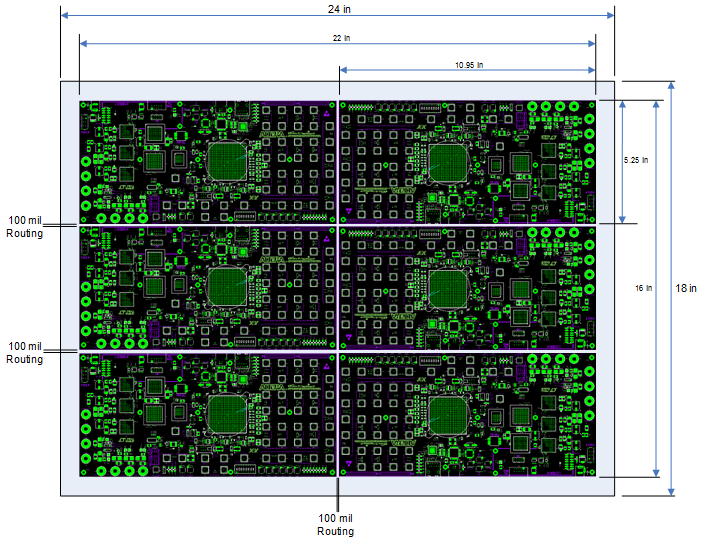
1.5. PCB Panelization
Always consider board panelization during the initial PCB sizing to maximize the number of board yield per PCB panel and reduce the cost per board. Although common PCB panel dimensions are 12 × 18 in and 18 × 24 in, the actual usable area left to the designer is typically one inch less on all sides of the panel. Therefore, the usable dimensions are 10 × 16 in and 16 × 22 in, respectively. Also, when panelizing multiple boards up on a PCB panel, the minimum spacing requirement between boards must be 100 mils to allow the individual boards to be routed out after fabrication. Below figure shows an example of maximum panel utilization on an 18 × 24 in panel. In this example, six Stratix IV GX SI development kit boards have been panelized as 6-up on a standard 18 × 24 in panel with 100 mil separation between adjacent boards to accommodate final routing of the board.
Figure 16. PCB Panelization