3.5. Cyclone® 10 LP EPE - I/O Worksheet
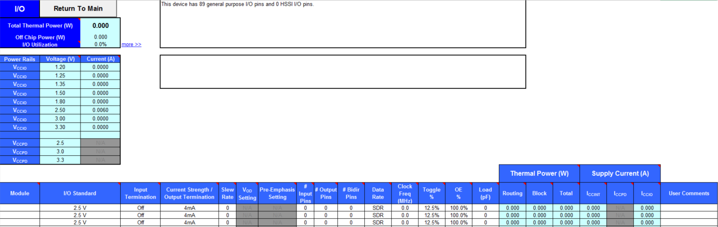
Each row in the I/O worksheet represents a design module where the I/O pins have the same I/O standard, input termination, current strength or output termination, data rate, clock frequency, output enable static probability, and capacitive load.
Enter the following parameters for each design module:
- I/O standard
- Input termination
- Current strength/Output termination
- Slew rate
- Differential output voltage (VOD) setting
- Pre-emphasis setting
- Number of input, output, and bidirectional pins
- I/O data rate
- Clock frequency (fMAX) (in MHz)
- Average pin toggle percentage
- Output enable static probability
- Capacitance of the load
For the EPE spreadsheet version 11.0 onwards, Off Chip Power (W) information is added into the I/O worksheet.
Figure 17. I/O Worksheet of the EPE Spreadsheet
When using the EPE spreadsheet, it is assumed you are using external termination resistors when you design with I/O standards that recommend termination resistors (SSTL and high-speed transceiver logic [HSTL]). If your design does not use external termination resistors, choose the LVTTL/LVCMOS I/O standard with the same VCCIO and similar current strength as the terminated I/O standard. For example, if you are using the SSTL-2 Class II I/O standard with a 16 mA current strength, you must select 2.5 V as the I/O standard and 16 mA as the current strength in the EPE spreadsheet.
To use on-chip termination (OCT), select the Current Strength/Output option in the EPE spreadsheet.
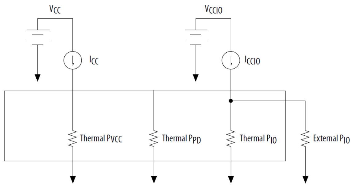
The power reported for the I/O signals includes thermal and external I/O power. The total thermal power is the sum of the thermal power consumed by the device from each power rail, as shown in the following equation.
Total Thermal Power = Thermal PVCC + Thermal PIO
The following figure shows the I/O power consumption. The ICCIO power rail includes both the thermal PIO and the external PIO.
Figure 18. I/O Power Representation
The VREF pins consume minimal current (typically less than 10 μA) and is negligible when compared with the current consumed by the general purpose I/O (GPIO) pins; therefore, the EPE spreadsheet does not include the current for VREF pins in the calculations.
| Column Heading | Description |
|---|---|
| Power Rails | Power supply rails for the I/O pins. |
| Voltage (V) | The voltage applied to the specified power rail in Volts (V). |
| Current (A) | The current drawn from the specified power rail in Amps (A). |
| Column Heading | Description |
|---|---|
| Module | Specify a name for the module in this column. This is an optional value. |
| I/O Buffer Settings | |
| I/O Standard | Select the I/O standard used for the input, output, or bidirectional pins in this module from the drop-down list. The calculated I/O power varies based on the I/O standard. For I/O standards that recommend termination (SSTL and HSTL), the EPE spreadsheet assumes you are using external termination resistors. If you are not using external termination resistors, choose the LVTTL/LVCMOS I/O standard with the same voltage and current strength as the terminated I/O standard. To view all the I/O standards in the drop-down list, use the scroll bar. |
| Input Termination | Select the input termination (on-chip parallel termination [RT OCT] or on-chip differential termination [RD OCT]) setting implemented for the input and bidirectional pins in this module. |
| Current Strength/ Output Termination | Select the current strength or output termination (on-chip serial termination [RS OCT]) implemented for the output and bidirectional pins in this module. Current strength and output termination are mutually exclusive. |
| Slew Rate | Select the slew rate setting for the output and bidirectional pins in this module. Using a lower slew rate setting helps to reduce switching noise but may increase delay. |
| VOD Setting | Select the VOD for the output and bidirectional pins in this module. If you use a lower voltage, it helps to reduce static power. |
| Pre-Emphasis Setting | Select the pre-emphasis setting for output and bidirectional pins in this module. Disable the pre-emphasis will reduce dynamic power. |
| #Input Pins | Enter the number of input pins used in this module. Consider a differential pin pair as one pin. |
| #Output Pins | Enter the number of output pins used in this module. Consider a differential pin pair as one pin. |
| #Bidir Pins | Enter the number of bidirectional pins used in this module. When you enable the output enable signal, the I/O pin is treated as an output. When you disable the output enable signal, the I/O pin is treated as an input. An I/O configured as bidirectional but used only as an output consumes more power than an I/O configured as output-only, due to the toggling of the input buffer every time the output buffer toggles (they share a common pin). |
| Data Rate | Select either SDR or DDR as the I/O data rate. This indicates whether the I/O value is updated once (single data rate [SDR]) or twice (double data rate [DDR]) in a clock cycle. If the data rate of the pin is DDR, it is possible to set the data rate to SDR and double the toggle percentage. The Quartus® Prime software uses this method to output information. |
| Clock Freq (MHz) | Enter the clock frequency (in MHz). This value is limited by the maximum frequency specification for the device family. 100 MHz with a 12.5% toggle means that each I/O pin toggles 12.5 million times per second (100 × 12.5%). |
| Toggle % | Enter the average percentage of input, output, and bidirectional pins toggling on each clock cycle. For input pins used as clocks, the toggle percentage ranges from 0 to 200% because clocks toggle at twice the frequency. If the pins use DDR circuitry, you can set the data rate to SDR and double the toggle percentage. The Quartus® Prime software uses this method to output information. Typically, the toggle percentage is 12.5%. To be more conservative, you can use a higher toggle percentage. |
| OE % |
Enter the average percentage of time that the:
During the remaining time the:
The value you enter must be a percentage between 0 and 100%. |
| Load (pF) | Enter the pin loading external to the chip (in pF). This only applies to outputs and bidirectional pins. Pin and package capacitance is already included in the I/O model. Therefore, only include the off-chip capacitance in the Load parameter. |
| Thermal Power (W)–Routing | This shows the power dissipation due to estimated routing (in watts). Routing power depends on placement-and-routing information, which is a function of design complexity. The values shown represent the routing power based on experimentation of more than 100 designs. For detailed analysis based on your design’s routing, use the Quartus® Prime Power Analyzer. This value is automatically calculated. |
| Thermal Power (W)–Block | This shows the power dissipation due to internal and load toggling of the I/O (in watts). For accurate analysis based on your design’s exact I/O configuration, use the Quartus® Prime Power Analyzer. This value is automatically calculated. |
| Thermal Power (W)–Total | This shows the total power dissipation (in watts). The total power dissipation is the sum of the routing and block power. This value is automatically calculated. |
| Supply Current (A)–ICC | This shows the current drawn from the VCC power rail and powers the internal digital circuitry. This value is automatically calculated. |
| Supply Current (A)–ICCIO | This shows the current drawn from the VCCIO power rail. Some of this current may be drawn into off-chip termination resistors. This value is automatically calculated. |
| User Comments | Enter any comments. This is an optional entry. |
For more information about I/O standard termination schemes, refer to the I/O Features section of the Cyclone® 10 LP device handbook.