Visible to Intel only — GUID: mwh1410979475826
Ixiasoft
1.4.2. Select the Controller Clock as Loan I/O
On the Peripheral Pins tab, scroll down to the Peripherals Mux Table to select the USB clock pin as loan I/O. This setting allows a clock from a PLL in the FPGA to connect to the USB controller.
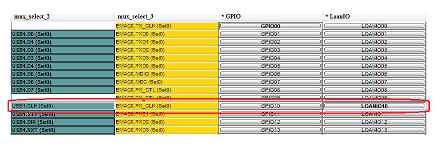
Refer to the following table for the appropriate loan I/O for each USB option.
| USB I/O Pin Set |
Loan I/O |
|---|---|
| USB0 I/O Set 0 | LOANIO44 |
| USB1 I/O Set 0 | LOANIO10 |
| USB1 I/O Set 1 | LOANIO29 |