Visible to Intel only — GUID: dlt1628537169299
Ixiasoft
1. Power Distribution Network
2. Gigahertz Channel Design Considerations
3. PCB and Stack-Up Design Considerations
4. Device Pin-Map, Checklists, and Connection Guidelines
5. General Board Design Considerations/Guidelines
6. Memory Interfacing Guidelines
7. Power Dissipation and Thermal Management
8. Tools, Models, and Libraries
9. Reference Designs and Development Kits
10. Document Revision History for AN 958: Board Design Guidelines
4.1. High Speed Board Design Advisor
4.2. Complete Pin Connection Table by Device
4.3. Pin Connection Guidelines By Device
4.4. Design for Debug with JTAG Pins
4.5. Hot Socketing, POR and Power Sequencing Support
4.6. Implementing OCT
4.7. Unused I/O Pins Guidelines
4.8. Device Breakout Guidelines
4.9. Additional Resources
5.1.1. Material Selection and Loss
5.1.2. Cross Talk Minimization
5.1.3. Power Filtering/Distribution
5.1.4. Unused I/O Pins
5.1.5. Signal Trace Routing
5.1.6. Ground Bounce
5.1.7. Understanding Transmission Lines
5.1.8. Impedance Calculation
5.1.9. Coplanar Wave Guides
5.1.10. Simultaneous Switching Noise Guidelines
Visible to Intel only — GUID: dlt1628537169299
Ixiasoft
1.5.5. Inter-Plane Capacitance
As a first-order analysis, the PCB power-ground plane pair can simply be modeled as a series connected resistor, inductor, and, capacitor as shown in Figure 6. Note that this simple model ignores the frequency dependent effects such as skin effect and dielectric absorption.
Figure 6. Simplified Impedance Model of the Power-Ground Plane Sandwich
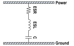
The first-order equations for the ESL in Figure 6 is shown below:
- ESL = (μ0•h•l)/w
Where,
- μ0 = magnetic permeability of free space (32 pH/mil)
- h = distance between the power and ground planes in mils
- l = length of the power plane in inches
- w = width of the power plane in inches
You can interpret the ESL of the power-ground plane sandwich as the spreading inductance that the decoupling capacitor sees as it is supplying current to the BGA device. Therefore, from the ESL equation above, the spreading inductance can be reduced by placing the decoupling capacitors as close as possible to the target BGA device (minimizing the distance l from the cap to the BGA device). Additionally, using a thin dielectric material (minimizing h) and wide plane pairs (maximize w) for the power-ground plane sandwich helps reduce the effective spreading inductance seen by the decoupling capacitor.