Visible to Intel only — GUID: doh1638499137139
Ixiasoft
1. About the Nios® V Embedded Processor
2. Nios® V Processor Hardware System Design with Intel® Quartus® Prime Software and Platform Designer
3. Nios® V Processor Software System Design
4. Nios® V Processor Configuration and Booting Solutions
5. Nios® V Processor - Using the MicroC/TCP-IP Stack
6. Nios® V Processor Debugging, Verifying, and Simulating
7. Nios® V Processor — Remote System Update
8. Nios® V Processor — Using Custom Instruction
9. Nios® V Embedded Processor Design Handbook Archives
10. Document Revision History for the Nios® V Embedded Processor Design Handbook
4.1. Introduction
4.2. Linking Applications
4.3. Nios® V Processor Booting Methods
4.4. Introduction to Nios® V Processor Booting Methods
4.5. Nios® V Processor Booting from Configuration QSPI Flash
4.6. Nios® V Processor Booting from On-Chip Memory (OCRAM)
4.7. Nios® V Processor Booting from Tightly Coupled Memory (TCM)
4.8. Summary of Nios® V Processor Vector Configuration and BSP Settings
6.5.1. Prerequisites
6.5.2. Setting Up and Generating Your Simulation Environment in Platform Designer
6.5.3. Creating Nios V Processor Software
6.5.4. Generating Memory Initialization File
6.5.5. Generating System Simulation Files
6.5.6. Running Simulation in the QuestaSim Simulator Using Command Line
Visible to Intel only — GUID: doh1638499137139
Ixiasoft
4.6.1.1. Hardware Design Flow
The following sections describe a step-by-step method for building a bootable system for a Nios® V processor application from OCRAM. The example below is built using Intel Arria 10 SoC development kit.
IP Component Settings
- Create your Nios® V processor project using Intel® Quartus® Prime and Platform Designer.
- Ensure the On-Chip Memory (RAM or ROM) Intel FPGA is added into your Platform Designer system.
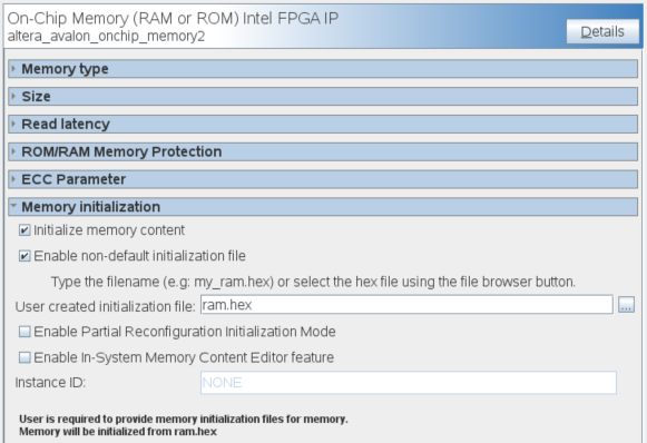
- Enable Initialize memory content and Enable non-default initialization file with ram.hex in the on-chip memory.
Figure 75. Connections for Nios® V Processor Project
Figure 76. On-Chip Memory (RAM or ROM) Intel FPGA IP Parameter Settings
Reset Agent Settings for Nios® V Processor
- In the Nios® V processor parameter editor, set the Reset Agent to OCRAM
Figure 77. Nios® V Processor Parameter Editor Settings
- Click Generate HDL, the Generation dialog box appears.
- Specify output file generation options and then click Generate.
Intel® Quartus® Prime Settings
- In the Intel Quartus Prime software, click Assignment > Device > Device and Pin Options > Configuration.
- Set Configuration scheme according to your FPGA configuration scheme
- Click OK to exit the Device and Pin Options window.
- Click OK to exit the Device window.
- Click Start Compilation to compile your project.
Related Information