Visible to Intel only — GUID: snz1474418824955
Ixiasoft
1.1. Reference Design Overview
1.2. Getting Started
1.3. Reference Design Components
1.4. Compiling the Reference Design
1.5. Testing the Reference Design
1.6. Extending the Reference Design with Custom Persona
1.7. Document Revision History for AN 784: Partial Reconfiguration over PCI Express* Reference Design for Intel® Arria® 10 Devices
Visible to Intel only — GUID: snz1474418824955
Ixiasoft
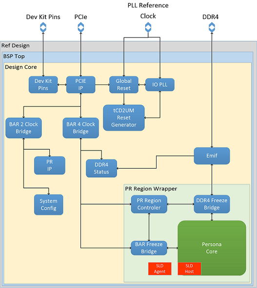
1.1. Reference Design Overview
The reference design consists of the following components:
- a10_pcie_reference_design—top-level wrapper for the reference design, connecting the board support package (BSP) subsystem to the device pins.
- bsp_top—top-level of the design that contains all subsystems of the design. This module consists of three main sub-components - the PCIe* IP core, the DDR4 External Memory Interfaces IP core, and the design top module. This layer of abstraction allows simulation of the design top module through simulated Avalon® Memory-Mapped ( Avalon® -MM) transactions.
- design_core—core of the design that handles generation of the PR region, the interface components such as clock crossing Avalon-MM logic and pipeline logic, clocks, and the global reset.
Figure 1. Intel® Arria® 10 PCIe* Reference Design Block Diagram