4.2. Arria® 10 EPE - Main Worksheet
The Main worksheet of the Early Power Estimator (EPE) for Arria® 10 allows you to enter device, package, and cooling information, and displays thermal power and thermal analysis information.
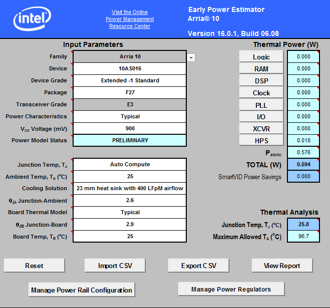
Figure 7. Arria® 10 EPE Main Worksheet
The required parameters depend on whether the junction temperature is manually entered or auto computed.
| Parameter | Description |
|---|---|
| Family | Select the device family. |
| Device | Select your device. Larger devices consume more static power and have higher clock dynamic power. All other power components are unaffected by device selection. |
| Device Grade | Select the combination of Operating Temperature, Speed Grade, and Power Option used.
|
| Package | Select the device package. Larger packages provide a larger cooling surface and more contact points to the circuit board, thus they offer lower thermal resistance. Package selection does not affect dynamic power directly. |
| Transceiver Grade | Select the transceiver grade.
Note: For information on transceiver grades, refer to Arria® 10 Device Variants and Packages, in the Arria® 10 Device Overview.
|
| Power Characteristics | Select typical or theoretical worst-case silicon process. There is a process variation from die-to-die. This variation primarily affects static power consumption. If you choose Typical power characteristics, estimates are based on average power consumed by typical silicon. For FPGA board power supply design, choose Maximum for worst-case values. To enable the Enpirion device selection, you must set the Power Characteristics to Maximum. |
| VCC Voltage (mV) | Select the voltage of the VCC power rail, in mV. |
| Power Model Status | Indicates whether the power model for the device is in preliminary or final status. Assuming accurate inputs to the Early Power Estimator, the margins for calculated current values are as described below:
|
| Junction Temp, TJ | Select whether Junction Temperature (TJ) should be computed automatically or provided by the user. |
| Ambient Temp, TA (°C)/Junction Temp, TJ (°C) | Enter the temperature of the air that is cooling the device. This value can range from –40°C to 125°C, depending on the device grade selected. If you turn on the Auto Compute junction temperature option, you can enter the ambient temperature in this field; otherwise, enter the actual junction temperature. |
| Cooling Solution | Select your cooling solution with associated airflow. (This field is not available when you enter the junction temperature directly.) Representative examples of heat sinks and airflows are provided; larger heat sinks provide lower thermal resistance, and thus lower junction temperature. If the heat sink and airflow is known, consult the data sheet, choose Custom, and in the θJA Junction-Ambient field, enter a junction to ambient value according to your system. |
| θJA Junction-Ambient | If you have specified a custom cooling solution, enter the Junction-Ambient value in °C/W. This value is used to compute the final junction temperature if you have selected Auto Compute (This field is not available when you enter the junction temperature directly.) |
| Board Thermal Model | This field is not applicable when no heat sink is used, or when you enter the junction temperature directly.
Select the type of board model to be used in thermal analysis. Available values are:
You should perform a detailed thermal simulation of your system to determine the final junction temperature. This two-resistor thermal model is for early estimation only. |
| θJB Junction-Board | If you specify a custom Board Thermal Model, enter the θJB Junction-Board value (in °C/W), in this field. (This field is not applicable when no heat sink is used, or when you enter the junction temperature directly.) |
| Board Temp, TB (°C) | If you specified a custom or typical Board Thermal Model, enter the board temperature to be used in thermal calculations (in °C). (This field is not applicable when no heat sink is used, or when you enter the junction temperature directly.) |
Thermal power is the power dissipated in the device. Total thermal power is the sum of the thermal power of all the resources used in the device, including the static, standby, and dynamic power. Total thermal power includes only the thermal component for the I/O worksheet and does not include external power dissipation, such as from voltage-referenced termination resistors.
The static power (PSTATIC) is the thermal power dissipated on the chip, independent of design activity. PSTATIC includes the static power from all FPGA functional blocks, except for I/O DC bias power and transceiver DC bias power, which are included in the standby power of the I/O and XCVR worksheets, respectively. PSTATIC is the only thermal power component that varies with junction temperature and power characteristics (process). PSTATIC is also the only thermal power component that varies significantly with selected device.
| Column Heading | Description |
|---|---|
| Logic | Displays the dynamic power consumed by adaptive logic modules (ALMs), flipflops (FFs) and associated routing. Click Logic to see details. |
| RAM | Displays the dynamic power consumed by RAMs and associated routing. Click RAM to see details. |
| DSP | Displays the dynamic power consumed by digital signal processing (DSP) blocks and associated routing. Click DSP to see details. |
| Clock | Displays the dynamic power consumed by clock networks. The clock dynamic power is affected by the selected device. Click Clock to see details. |
| PLL | Displays the dynamic power consumed by phase-locked loops (PLLs). Click PLL to see details. |
| I/O | Displays the thermal power consumed by I/O pins and I/O subsystems. Click I/O to see details. |
| XCVR | Displays the total power consumed by transceiver blocks. Click XCVR to see details. |
| HPS | Displays the total power consumed by the hard processor system (HPS). Click HPS to see details. |
| Pstatic | Displays the static power consumed regardless of clock frequency. This includes static power consumed by I/O and transceiver blocks, but does not include standby power. Pstatic is affected by junction temperature, selected device, power characteristics, and M20K, DSP and high speed LAB usage.
Note: For information on measuring the static power consumption of a specific device, refer to the appendix Measuring Static Power.
|
| TOTAL (W) | Displays the total power dissipated as heat from the FPGA. This value includes power savings due to SmartVID. This value does not include power dissipated in off-chip termination resistors. Total power dissipation in the FPGA may differ from the sum of power on all rails due to several factors including, but not limited to, the power dissipated in off-chip termination resistors. Refer to the Report worksheet for power supply currents drawn from the FPGA supply rails. |
| SmartVID Power Savings | Displays the total power reduction (static and dynamic) resulting from the lower voltage that is made possible by SmartVID. This power reduction is dependent on the user design and device characteristics. The combination of these factors may result in different static and dynamic power savings, so the exact dynamic and static components are not identified separately, and the power reduction reported here is a worst-case result. This field is applicable only to devices that support the SmartVID feature, and only if the SmartVoltage ID setting is set to On. The SmartVID Power Savings value is provided for informational purposes only; the savings due to SmartVID are already included in the TOTAL (W) value. |
Note: If any thermal power value is highlighted in red, it indicates an error in the design specification. Review the relevant worksheet for errors or utilization values exceeding 100%. Correct any errors to obtain reliable power and temperature estimates.
The Thermal Analysis section displays the junction temperature (TJ) and the maximum allowed ambient temperature (TA) values.
| Column Heading | Description |
|---|---|
| Junction Temp, TJ (°C) | If you specified a value for Junction Temp (TJ), the value in this field is equal to the value that you specified. If you specified Auto Compute for Junction Temp (TJ), this field displays the estimated device junction temperature based on the thermal parameters provided. The junction temperature is determined by dissipating the total thermal power through the top of the chip and through the board. |
| Maximum Allowed TA (°C) / Maximum Allowed TJ (C) | If you specified a value for Junction Temp (TJ), the value in this field is the maximum allowable device junction temperature (in °C), based on the specified device grade. If you specified Auto Compute for Junction Temp (TJ), this field provides a guideline for the maximum ambient temperature (in °C) to which the device can be subjected, without exceeding the maximum allowable junction temperature, based on the specified cooling solution and device grade. |
You can directly enter or automatically compute the junction temperature based on the information provided. To enter the junction temperature, select User Entered in the Junction Temp field in the Input Parameters section. To automatically compute the junction temperature, select Auto Compute in the same field.
When automatically computing the junction temperature, the ambient temperature, cooling solution, board thermal model, and board temperature of the device determine the junction temperature in °C. Junction temperature is the estimated operating junction temperature based on your device and thermal conditions.
You can consider the device as a heat source and the junction temperature is the temperature of the device. While the temperature typically varies across the device, to simplify the analysis, you can assume that the temperature of the device is constant regardless of where it is measured.
Power from the device can be dissipated through different paths. Different paths become significant depending on the thermal properties of the system. The significance of power dissipation paths vary depending on whether or not a heat sink is used for the device.
Not Using a Heatsink
When you do not use a heat sink, the major paths of power dissipation are from the device to the air. You can refer to this as a junction-to-ambient thermal resistance. In this case, there are two significant junction-to-ambient thermal resistance paths:
- From the device through the case to the air
- From the device to the board
Figure 8. Thermal Representation without a Heat Sink
In the model used in the EPE spreadsheet, power is dissipated through the case and board. The θJA values are calculated for differing air flow options accounting for the paths through the case and through the board.
Figure 9. Thermal Model in the EPE Spreadsheet without a Heat Sink
The ambient temperature does not change, but the junction temperature changes depending on the thermal properties and total power dissipation, which in turn is affected by junction temperature. The junction temperature calculation is an iterative process.
The following equation shows the total power calculated based on the total θJA value, ambient, and junction temperatures.
When you use a heat sink, the major paths of power dissipation are from the device through the case, thermal interface material, and heat sink. There is also a path of power dissipation through the board. The path through the board has less impact than the path to air.
Figure 10. Thermal Representation with a Heat Sink
In the model used in the EPE spreadsheet, power is dissipated through the board and through the case and heat sink. The junction-to-board thermal resistance (θJB) refers to the thermal resistance of the path through the board. Junction-to-ambient thermal resistance (θJA) refers to the thermal resistance of the path through the case, thermal interface material, and heat sink.
Figure 11. Thermal Model for the EPE Spreadsheet with a Heat Sink
If you want the EPE spreadsheet thermal model to take the θJB into consideration, set the Board Thermal Model parameter to either Typical or Custom. Otherwise, set the Board Thermal Model parameter to None (conservative). In this case, the path through the board is not considered for power dissipation and a more conservative thermal power estimate is obtained.
The addition of the junction-to-case thermal resistance (θJC), the case-to-heat sink thermal resistance (θCS) and the heat sink-to-ambient thermal resistance (θSA) determines the θJA, as shown by the following equation.
Based on the device, package, airflow, and heat sink solution selected in the Input Parameters section, the EPE spreadsheet determines the θJA.
If you use a low, medium, or high profile heat sink, select the airflow from the values of Still Air and air flow rates of 100 lfm (0.5 m/s), 200 lfm (1.0 m/s), and 400 lfm (2.0 m/s). If you use a custom cooling solution, enter the custom θJA value. You must incorporate the airflow and junction to case resistance into the custom θJA value. You can obtain these values from the heat sink manufacturer.
The ambient temperature does not change, but the junction temperature changes depending on the thermal properties. Calculating the junction temperature is an iterative process because a change in junction temperature affects the thermal device properties, due to a change in power dissipation. Those thermal device properties are used to calculate junction temperature.
The total power is calculated based on the θJA and θJBvalues, and ambient board and junction temperatures with the following equation.
| Button Name | Description |
|---|---|
| Logic | Opens the Logic worksheet to display details of the dynamic power consumed by adaptive logic modules (ALMs), flipflops, and associated routing. |
| RAM | Opens the RAM worksheet to display details of the dynamic power consumed by RAMs and associated routing. |
| DSP | Opens the DSP worksheet to display details of the dynamic power consumed by digital signal processing blocks and associated routing. |
| Clock | Opens the Clock worksheet to display details of the dynamic power consumed by clock networks and associated routing. |
| PLL | Opens the PLL worksheet to display details of the dynamic power consumed by phase-locked loops and associated routing. |
| I/O | Opens the I/O worksheet to display details of the thermal power consumed by I/O pins and I/O subsystems. |
| XCVR | Opens the XCVR worksheet to display details of the total power consumed by transceiver blocks. |
| HPS | Opens the HPS worksheet to display details of the total power consumed by the hard processor system (HPS). |
| Reset | Resets the Early Power Estimator to default values; any parameters that you have specified are lost. |
| Import CSV | Allows you to import parameters from a comma-separated value file. |
| Export CSV | Allows you to export parameters to a comma-separated value file. |
| View Report | Displays the Report worksheet. |
| Manage Power Rail Configuration | Displays the Power Rail Configuration table, on the Report worksheet. |
| Manage Power Regulators | Displays the Regulator Selection table, on the Enpirion worksheet. |