Visible to Intel only — GUID: hpg1547062935061
Ixiasoft
1. About the External Memory Interfaces Agilex™ 7 F-Series and I-Series FPGA IP
2. Agilex™ 7 F-Series and I-Series FPGA EMIF IP – Introduction
3. Agilex™ 7 F-Series and I-Series FPGA EMIF IP – Product Architecture
4. Agilex™ 7 F-Series and I-Series FPGA EMIF IP – End-User Signals
5. Agilex™ 7 F-Series and I-Series FPGA EMIF IP – Simulating Memory IP
6. Agilex™ 7 F-Series and I-Series FPGA EMIF IP – DDR4 Support
7. Agilex™ 7 F-Series and I-Series FPGA EMIF IP – QDR-IV Support
8. Agilex™ 7 F-Series and I-Series FPGA EMIF IP – Timing Closure
9. Agilex™ 7 F-Series and I-Series FPGA EMIF IP – I/O Timing Closure
10. Agilex™ 7 F-Series and I-Series FPGA EMIF IP – Controller Optimization
11. Agilex™ 7 F-Series and I-Series FPGA EMIF IP – Debugging
12. External Memory Interfaces Agilex™ 7 F-Series and I-Series FPGA IP User Guide Archives
13. Document Revision History for External Memory Interfaces Agilex™ 7 F-Series and I-Series FPGA IP User Guide
3.1. Intel® Agilex™ 7 F-Series and I-Series EMIF Architecture: Introduction
3.2. Intel® Agilex™ 7 F-Series and I-Series EMIF Sequencer
3.3. Intel® Agilex™ 7 F-Series and I-Series EMIF Calibration
3.4. Intel® Agilex™ 7 F-Series and I-Series EMIF Controller
3.5. User-requested Reset in Intel® Agilex™ 7 F-Series and I-Series EMIF IP
3.6. Intel® Agilex™ 7 F-Series and I-Series EMIF for Hard Processor Subsystem
3.7. Using a Custom Controller with the Hard PHY
3.1.1. Intel® Agilex™ 7 F-Series and I-Series EMIF Architecture: I/O Subsystem
3.1.2. Intel® Agilex™ 7 F-Series and I-Series EMIF Architecture: I/O SSM
3.1.3. Intel® Agilex™ 7 F-Series and I-Series EMIF Architecture: I/O Bank
3.1.4. Intel® Agilex™ 7 F-Series and I-Series EMIF Architecture: I/O Lane
3.1.5. Intel® Agilex™ 7 F-Series and I-Series EMIF Architecture: Input DQS Clock Tree
3.1.6. Intel® Agilex™ 7 F-Series and I-Series EMIF Architecture: PHY Clock Tree
3.1.7. Intel® Agilex™ 7 F-Series and I-Series EMIF Architecture: PLL Reference Clock Networks
3.1.8. Intel® Agilex™ 7 F-Series and I-Series EMIF Architecture: Clock Phase Alignment
3.3.4.3.1. Debugging Calibration Failure Using Information from the Calibration report
3.3.4.3.2. Debugging Address and Command Leveling Calibration Failure
3.3.4.3.3. Debugging Address and Command Deskew Failure
3.3.4.3.4. Debugging DQS Enable Failure
3.3.4.3.5. Debugging Read Deskew Calibration Failure
3.3.4.3.6. Debugging VREFIN Calibration Failure
3.3.4.3.7. Debugging LFIFO Calibration Failure
3.3.4.3.8. Debugging Write Leveling Failure
3.3.4.3.9. Debugging Write Deskew Calibration Failure
3.3.4.3.10. Debugging VREFOUT Calibration Failure
4.1. Intel® Agilex™ 7 F-Series and I-Series EMIF IP Interface and Signal Descriptions
4.2. Intel® Agilex™ 7 F-Series and I-Series EMIF IP AFI Signals
4.3. Intel® Agilex™ 7 F-Series and I-Series EMIF IP AFI 4.0 Timing Diagrams
4.4. Intel® Agilex™ 7 F-Series and I-Series EMIF IP Memory Mapped Register (MMR) Tables
4.1.1.1. local_reset_req for DDR4
4.1.1.2. local_reset_status for DDR4
4.1.1.3. pll_ref_clk for DDR4
4.1.1.4. pll_locked for DDR4
4.1.1.5. ac_parity_err for DDR4
4.1.1.6. oct for DDR4
4.1.1.7. mem for DDR4
4.1.1.8. status for DDR4
4.1.1.9. afi_reset_n for DDR4
4.1.1.10. afi_clk for DDR4
4.1.1.11. afi_half_clk for DDR4
4.1.1.12. afi for DDR4
4.1.1.13. emif_usr_reset_n for DDR4
4.1.1.14. emif_usr_clk for DDR4
4.1.1.15. ctrl_amm for DDR4
4.1.1.16. ctrl_amm_aux for DDR4
4.1.1.17. ctrl_auto_precharge for DDR4
4.1.1.18. ctrl_user_priority for DDR4
4.1.1.19. ctrl_ecc_user_interrupt for DDR4
4.1.1.20. ctrl_ecc_readdataerror for DDR4
4.1.1.21. ctrl_ecc_status for DDR4
4.1.1.22. ctrl_mmr_slave for DDR4
4.1.1.23. hps_emif for DDR4
4.1.1.24. emif_calbus for DDR4
4.1.1.25. emif_calbus_clk for DDR4
4.1.2.1. local_reset_req for QDR-IV
4.1.2.2. local_reset_status for QDR-IV
4.1.2.3. pll_ref_clk for QDR-IV
4.1.2.4. pll_locked for QDR-IV
4.1.2.5. oct for QDR-IV
4.1.2.6. mem for QDR-IV
4.1.2.7. status for QDR-IV
4.1.2.8. afi_reset_n for QDR-IV
4.1.2.9. afi_clk for QDR-IV
4.1.2.10. afi_half_clk for QDR-IV
4.1.2.11. afi for QDR-IV
4.1.2.12. emif_usr_reset_n for QDR-IV
4.1.2.13. emif_usr_clk for QDR-IV
4.1.2.14. ctrl_amm for QDR-IV
4.1.2.15. emif_calbus for QDR-IV
4.1.2.16. emif_calbus_clk for QDR-IV
4.4.1. ctrlcfg0
4.4.2. ctrlcfg1
4.4.3. dramtiming0
4.4.4. sbcfg1
4.4.5. caltiming0
4.4.6. caltiming1
4.4.7. caltiming2
4.4.8. caltiming3
4.4.9. caltiming4
4.4.10. caltiming9
4.4.11. dramaddrw
4.4.12. sideband0
4.4.13. sideband1
4.4.14. sideband4
4.4.15. sideband6
4.4.16. sideband7
4.4.17. sideband9
4.4.18. sideband11
4.4.19. sideband12
4.4.20. sideband13
4.4.21. sideband14
4.4.22. dramsts
4.4.23. niosreserve0
4.4.24. niosreserve1
4.4.25. sideband16
4.4.26. ecc3: ECC Error and Interrupt Configuration
4.4.27. ecc4: Status and Error Information
4.4.28. ecc5: Address of Most Recent SBE/DBE
4.4.29. ecc6: Address of Most Recent Correction Command Dropped
4.4.30. ecc7: Extension for Address of Most Recent SBE/DBE
4.4.31. ecc8: Extension for Address of Most Recent Correction Command Dropped
6.1. Intel® Agilex™ 7 F-Series and I-Series FPGA EMIF IP Parameter Descriptions
6.2. Intel® Agilex™ 7 F-Series and I-Series External Memory Interfaces Intel® Calibration IP Parameters
6.3. Register Map IP-XACT Support for Intel® Agilex™ 7 F-Series and I-Series EMIF DDR4 IP
6.4. Intel® Agilex™ 7 F-Series and I-Series FPGA EMIF IP Pin and Resource Planning
6.5. DDR4 Board Design Guidelines
6.1.1. Intel® Agilex™ 7 F-Series and I-Series EMIF IP DDR4 Parameters: General
6.1.2. Intel® Agilex™ 7 F-Series and I-Series EMIF IP DDR4 Parameters: Memory
6.1.3. Intel® Agilex™ 7 F-Series and I-Series EMIF IP DDR4 Parameters: Mem I/O
6.1.4. Intel® Agilex™ 7 F-Series and I-Series EMIF IP DDR4 Parameters: FPGA I/O
6.1.5. Intel® Agilex™ 7 F-Series and I-Series EMIF IP DDR4 Parameters: Mem Timing
6.1.6. Intel® Agilex™ 7 F-Series and I-Series EMIF IP DDR4 Parameters: Controller
6.1.7. Intel® Agilex™ 7 F-Series and I-Series EMIF IP DDR4 Parameters: Diagnostics
6.1.8. Intel® Agilex™ 7 F-Series and I-Series EMIF IP DDR4 Parameters: Example Designs
6.5.1. Terminations for DDR4 with Intel® Agilex™ 7 F-Series and I-Series Devices
6.5.2. Clamshell Topology
6.5.3. General Layout Routing Guidelines
6.5.4. Reference Stackup
6.5.5. Intel® Agilex™ 7 F-Series and I-Series EMIF-Specific Routing Guidelines for Various DDR4 Topologies
6.5.6. DDR4 Routing Guidelines: Discrete (Component) Topologies
6.5.7. Intel® Agilex™ 7 F-Series and I-Series EMIF Pin Swapping Guidelines
6.5.5.1. One DIMM per Channel (1DPC) for UDIMM, RDIMM, LRDIMM, and SODIMM DDR4 Topologies
6.5.5.2. Two DIMMs per Channel (2DPC) for UDIMM, RDIMM, and LRDIMM DDR4 Topologies
6.5.5.3. Two DIMMs per Channel (2DPC) for SODIMM Topology
6.5.5.4. Skew Matching Guidelines for DIMM Configurations
6.5.5.5. Power Delivery Recommendations for the Memory / DIMM Side
6.5.6.1. Single Rank x 8 Discrete (Component) Topology
6.5.6.2. Single Rank x 16 Discrete (Component) Topology
6.5.6.3. ADDR/CMD Reference Voltage/RESET Signal Routing Guidelines for Single Rank x 8 and R Rank x 16 Discrete (Component) Topologies
6.5.6.4. Skew Matching Guidelines for DDR4 Discrete Configurations
6.5.6.5. Power Delivery Recommendations for DDR4 Discrete Configurations
7.1.1. Intel® Agilex™ 7 F-Series and I-Series EMIF IP QDR-IV Parameters: General
7.1.2. Intel® Agilex™ 7 F-Series and I-Series EMIF IP QDR-IV Parameters: Memory
7.1.3. Intel® Agilex™ 7 F-Series and I-Series EMIF IP QDR-IV Parameters: FPGA I/O
7.1.4. Intel® Agilex™ 7 F-Series and I-Series EMIF IP QDR-IV Parameters: Mem Timing
7.1.5. Intel® Agilex™ 7 F-Series and I-Series EMIF IP QDR-IV Parameters: Controller
7.1.6. Intel® Agilex™ 7 F-Series and I-Series EMIF IP QDR-IV Parameters: Diagnostics
7.1.7. Intel® Agilex™ 7 F-Series and I-Series EMIF IP QDR-IV Parameters: Example Designs
7.3.3.1. Intel® Agilex™ 7 F-Series and I-Series FPGA EMIF IP Banks
7.3.3.2. General Guidelines
7.3.3.3. QDR IV SRAM Commands and Addresses, AP, and AINV Signals
7.3.3.4. QDR IV SRAM Clock Signals
7.3.3.5. QDR IV SRAM Data, DINV, and QVLD Signals
7.3.3.6. Specific Pin Connection Requirements
7.3.3.7. Resource Sharing Guidelines (Multiple Interfaces)
9.1. I/O Timing Closure Overview
9.2. Collateral Generated with Your EMIF IP
9.3. SPICE Decks
9.4. File Organization
9.5. Top-level Parameterization File
9.6. IP-Supplied Parameters that You Might Need to Override
9.7. Understanding the *_ip_parameters.dat File and Making a Mask Polygon
9.8. Multi-Rank Topology
9.9. Pin Parasitics
9.10. Mask Evaluation
10.4.1. Auto-Precharge Commands
10.4.2. Additive Latency
10.4.3. Bank Interleaving
10.4.4. Additive Latency and Bank Interleaving
10.4.5. User-Controlled Refresh
10.4.6. Frequency of Operation
10.4.7. Series of Reads or Writes
10.4.8. Data Reordering
10.4.9. Starvation Control
10.4.10. Command Reordering
10.4.11. Bandwidth
10.4.12. Enable Command Priority Control
10.4.13. Controller Pre-pay and Post-pay Refresh (DDR4 Only)
11.1. Interface Configuration Performance Issues
11.2. Functional Issue Evaluation
11.3. Timing Issue Characteristics
11.4. Verifying Memory IP Using the Signal Tap Logic Analyzer
11.5. Hardware Debugging Guidelines
11.6. Categorizing Hardware Issues
11.7. Debugging with the External Memory Interface Debug Toolkit
11.8. Using the Default Traffic Generator
11.9. Using the Configurable Traffic Generator (TG2)
11.10. EMIF On-Chip Debug Port
11.11. Efficiency Monitor
11.5.1. Create a Simplified Design that Demonstrates the Same Issue
11.5.2. Measure Power Distribution Network
11.5.3. Measure Signal Integrity and Setup and Hold Margin
11.5.4. Vary Voltage
11.5.5. Operate at a Lower Speed
11.5.6. Determine Whether the Issue Exists in Previous Versions of Software
11.5.7. Determine Whether the Issue Exists in the Current Version of Software
11.5.8. Try A Different PCB
11.5.9. Try Other Configurations
11.5.10. Debugging Checklist
11.7.4.3.1. Debugging Calibration Failure Using Information from the Calibration report
11.7.4.3.2. Debugging Address and Command Leveling Calibration Failure
11.7.4.3.3. Debugging Address and Command Deskew Failure
11.7.4.3.4. Debugging DQS Enable Failure
11.7.4.3.5. Debugging Read Deskew Calibration Failure
11.7.4.3.6. Debugging VREFIN Calibration Failure
11.7.4.3.7. Debugging LFIFO Calibration Failure
11.7.4.3.8. Debugging Write Leveling Failure
11.7.4.3.9. Debugging Write Deskew Calibration Failure
11.7.4.3.10. Debugging VREFOUT Calibration Failure
11.9.1. Enabling the Traffic Generator in a Design Example
11.9.2. Traffic Generator Block Description
11.9.3. Default Traffic Pattern
11.9.4. Configuration and Status Registers
11.9.5. User Pattern
11.9.6. Traffic Generator Status
11.9.7. Starting Traffic with the Traffic Generator
11.9.8. Traffic Generator Configuration User Interface
Visible to Intel only — GUID: hpg1547062935061
Ixiasoft
3.1.8. Intel® Agilex™ 7 F-Series and I-Series EMIF Architecture: Clock Phase Alignment
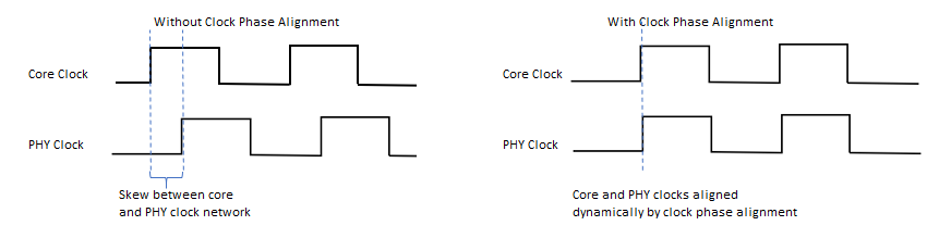
In Intel® Agilex™ 7 F-Series and I-Series external memory interfaces, a global clock network clocks registers inside the FPGA core, and the PHY clock network clocks registers inside the FPGA periphery. Clock phase alignment circuitry employs negative feedback to dynamically adjust the phase of the core clock signal to match the phase of the PHY clock signal.
The clock phase alignment feature effectively eliminates the clock skew effect in all transfers between the core and the periphery, facilitating timing closure. All Intel® Agilex™ 7 F-Series and I-Series external memory interfaces employ clock phase alignment circuitry.
Figure 54. Clock Phase Alignment Illustration
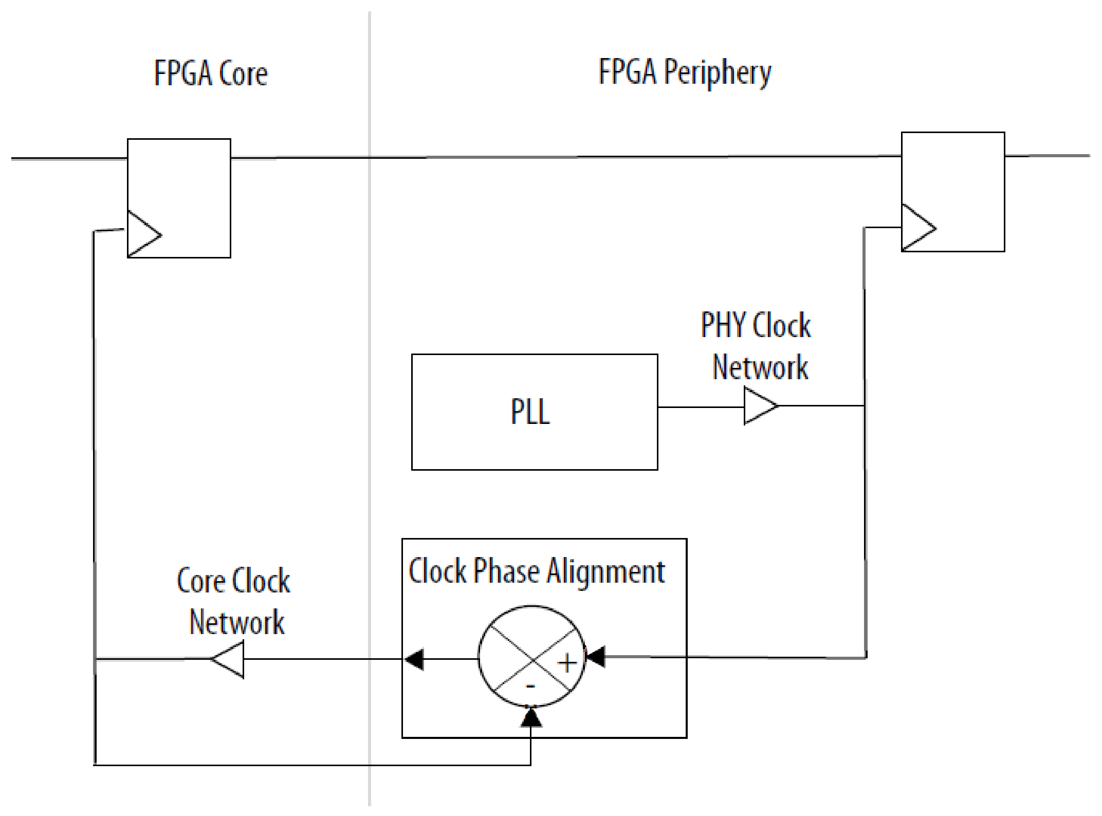
Figure 55. Effect of Clock Phase Alignment